Introduction
Building a 4-bit calculator is a fun and educational project that can help you to understand the basic principles of digital logic design. In this project, we will be using Proteus 8 software to simulate the circuit design and test it before building the physical calculator. The calculator will be able to perform addition, subtraction, multiplication, and division operations using logic gates and a 7-segment display.Project Overview
The 4-bit calculator project consists of three main components: the input circuit, the logic circuit, and the output circuit. The input circuit is responsible for taking in the user input, the logic circuit processes the input and performs the necessary calculations, and the output circuit displays the result on a 7-segment display.The Input Circuit
The input circuit consists of four push buttons that represent the four bits of the input number. Each button is connected to a pull-down resistor to ensure that the input is at a known state when the button is not pressed. The input circuit also includes a fifth push button to select the operation to be performed.The Logic Circuit
The logic circuit is the heart of the calculator and performs the arithmetic operations on the input numbers. We will use logic gates such as AND, OR, XOR, and NOT gates to perform the operations. We will also use a binary adder and a binary subtractor to perform addition and subtraction operations respectively. The output of the logic circuit is a four-bit binary number that represents the result of the operation.The Output Circuit
The output circuit consists of a 7-segment display that is used to display the result of the operation. The display is made up of seven segments labeled A to G and a decimal point. Each segment is connected to a transistor through a resistor. The transistors are controlled by the output of the logic circuit to display the correct number on the display.Designing the Input Circuit
To design the input circuit, we will use four push buttons and a fifth button to select the operation to be performed. Each button will be connected to a pull-down resistor to ensure that the input is at a known state when the button is not pressed. The button connections will be connected to a 4-bit binary encoder to encode the input numbers into binary format.Designing the Logic Circuit
The logic circuit is designed using logic gates and binary adder and subtractor circuits. The addition and subtraction circuits are designed using full adder and full subtractor circuits respectively. The output of the logic circuit is a four-bit binary number that represents the result of the operation.Designing the Output Circuit
The output circuit is designed using a 7-segment display that is used to display the result of the operation. The display is made up of seven segments labeled A to G and a decimal point. Each segment is connected to a transistor through a resistor. The transistors are controlled by the output of the logic circuit to display the correct number on the display.Simulating the Circuit in Proteus 8
Proteus 8 software allows you to simulate and test the circuit design before building the physical calculator. The software provides a wide range of simulation tools that enable you to test and debug the circuit design. Once you have designed the input, logic, and output circuits, you can simulate the circuit in Proteus 8 and test the functionality of the calculator.Implementation
1 & 2. Adder/Subtractor Circuit
An adder/subtractor circuit is an electronic circuit that can perform both addition and subtraction of binary numbers. It is a basic arithmetic circuit that can be used in various digital systems such as computers, calculators, and more.
The circuit consists of two inputs: A and B. A and B represent the binary numbers that need to be added or subtracted. The circuit also has two control inputs: CIN and MODE. CIN represents the carry-in input for the adder, and MODE determines whether the circuit performs addition or subtraction.
When MODE is set to 0, the circuit performs addition. In this case, the output of the circuit is the sum of A, B, and the carry-in input, if any. The carry-out output of the adder is used as the carry-in input of the next bit in the circuit.
When MODE is set to 1, the circuit performs subtraction. In this case, the output of the circuit is the difference between A and B. The borrow output of the subtractor is used as the carry-in input of the next bit in the circuit.
The adder/subtractor circuit can be built using various logic gates such as XOR, AND, OR, and NOT gates. The circuit can be designed using digital design software such as Proteus, Logisim, or VHDL.
Overall, an adder/subtractor circuit is a useful circuit that can perform both addition and subtraction of binary numbers. It is an important component of digital systems and is widely used in various applications.
The full adder circuit consists of three inputs: A, B, and CIN. A and B are the two binary digits to be added, while CIN is the carry from the previous addition. The circuit also has two outputs: SUM and COUT. SUM is the sum of A, B, and CIN, while COUT is the carry-out from the addition.
The full adder circuit can be built using various logic gates such as XOR, AND, and OR gates. One common implementation of the full adder circuit is to use two half adders and an OR gate. The half adder adds two binary digits without a carry input.The first half adder adds A and B, resulting in a partial sum and a carry. The second half adder adds the partial sum from the first half adder, along with CIN. The final sum and carry are obtained from the second half adder.The full adder circuit is an essential component of digital systems and is widely used in various applications. It can be designed using digital design software such as Proteus, Logisim, or VHDL.
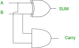
The half adder circuit can be built using various logic gates such as XOR and AND gates. The XOR gate produces the sum of the two inputs, while the AND gate produces the carry-out.In the half adder circuit, the XOR gate is used to produce the SUM output. The AND gate produces the CARRY output. If both A and B are 1, then the carry-out is 1. Otherwise, the carry-out is 0.
Multiplier Circuit
The logic gate multiplier circuit consists of two inputs: multiplicand and multiplier. The multiplicand is the number being multiplied, and the multiplier is the number by which the multiplicand is multiplied. The circuit also has two outputs: product and carry. The product is the result of the multiplication, while the carry represents any carry bits produced during the multiplication.
The logic gate multiplier circuit can be designed using various logic gates such as AND, XOR, and OR gates. One common implementation of the logic gate multiplier circuit is the Wallace tree multiplier, which uses a series of AND and XOR gates to perform the multiplication.
In the Wallace tree multiplier, the multiplicand is multiplied by each bit of the multiplier. The partial products obtained from each multiplication are then added together using a series of XOR gates. The resulting sum is then fed through a series of compressors, which further reduces the number of partial products to produce the final product.
Binary Unsigned Divider Algorithm
The binary unsigned divider algorithm is a method for dividing two binary numbers without considering their sign. It is a fundamental component in digital arithmetic and is widely used in various applications such as signal processing, cryptography, and more.
- The binary unsigned divider algorithm consists of the following steps:
- Compare the dividend (the number being divided) to the divisor (the number by which the dividend is divided) and determine the number of bits in the quotient (the result of the division).
- Initialize the quotient and remainder to zero.
- For each bit in the quotient (starting from the leftmost bit), perform the following sub-steps:
- Shift the remainder and the next bit of the dividend (starting from the leftmost bit) to the left by one bit.
- Subtract the divisor from the shifted remainder. If the result is non-negative, set the corresponding bit in the quotient to one and leave the remainder as it is. Otherwise, leave the corresponding bit in the quotient as zero and restore the remainder by adding the divisor back to it.
- The final quotient is the result of the division, and the remainder is the remainder of the division.
The binary unsigned divider algorithm is an essential component of digital systems and is widely used in various applications.
Tested Cases
Summation
7 + 5 -> C (12 in Decimal)
Subtraction
F (15 in Decimal) - 6 = 9
Multiplication
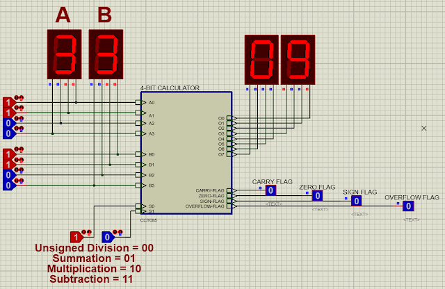
3 * 3 = 9
Division
B (11 in Decimal) / 3:
The remainder of Division: 2
Quotient of Division: 3


